Home › JEE Main 2025 Jan Physics PYQ › Semiconductors & Communication

JEE Main 2025 January Physics: Semiconductors & Communication – Previous Year Questions

All 10 questions asked from Semiconductors & Communication in JEE Main 2025 January Physics (22, 23, 24, 28 and 29 January, all shifts). This chapter is about 4.0% of the 250 Physics questions in the session: 10 single-correct (MCQ) and 0 numerical-value questions. Select an answer to attempt each question, and open “View solution” under it.

10questions
10MCQ
0numerical
4.0%of Physics paper

Topics asked in this chapter

  • Diodes & Junction Devices – 3 questions
  • Logic Gates – 3 questions
  • Semiconductor Devices & Communication – 4 questions

Diodes & Junction Devices

Q122 Jan 2025 · Shift 1MCQ
Which of the following circuits represents a forward biased diode?
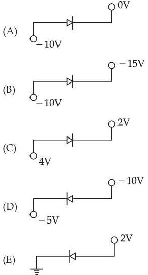
Figure for the question
Choose the correct answer from the options given below :
  1. A
    (B), (D) and (E) only
  2. B
    (C) and (E) only
  3. C
    (B), (C) and (E) only
  4. D
    (A) and (D) only
Q224 Jan 2025 · Shift 1MCQ
Consider the following statements:
A. The junction area of solar cell is made very narrow compared to a photo diode.
B. Solar cells are not connected with any external bias.
C. LED is made of lightly doped p-n junction.
D. Increase of forward current results in continuous increase of LED light intensity.
E. LEDs have to be connected in forward bias for emission of light.
Choose the correct answer from the options given below:
  1. A
    B, D, E Only
  2. B
    A, C, E Only
  3. C
    B, E Only
  4. D
    A, C Only
Q328 Jan 2025 · Shift 2MCQ
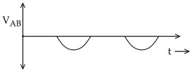
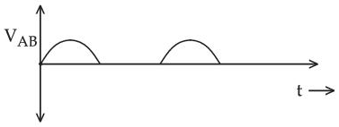
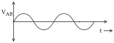
In the circuit shown here, assuming threshold voltage of diode is negligibly small, then voltage $V_{AB}$ is correctly represented by :
  1. A
    Figure for the question
  2. B
    Figure for the question
  3. C
    Figure for the question
  4. D
    $V_{AB}$ would be zero at all times

Logic Gates

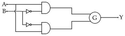
Q422 Jan 2025 · Shift 2MCQ
Figure for the question
ABY
001
010
100
111
To obtain the given truth table, following logic gate should be placed at G :
  1. A
    AND Gate
  2. B
    NOR Gate
  3. C
    OR Gate
  4. D
    NAND Gate
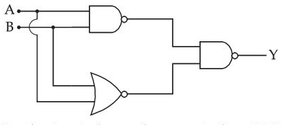
Q529 Jan 2025 · Shift 1MCQ
For the circuit shown above, equivalent GATE is :
Figure for the question
  1. A
    AND gate
  2. B
    NOT gate
  3. C
    OR gate
  4. D
    NAND gate
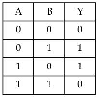
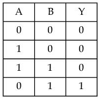
Q629 Jan 2025 · Shift 2MCQ
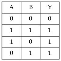
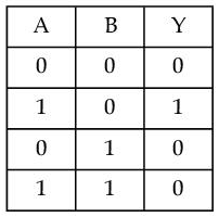
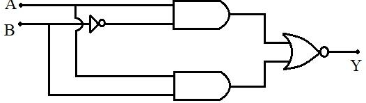
The truth table for the circuit given below is :
Figure for the question
  1. A
    Figure for the question
  2. B
    Figure for the question
  3. C
    Figure for the question
  4. D
    Figure for the question

Semiconductor Devices & Communication

Q723 Jan 2025 · Shift 2MCQ
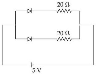
What is the current through the battery in the circuit shown below ?
Figure for the question
  1. A
    0.25 A
  2. B
    1.0 A
  3. C
    1.5 A
  4. D
    0.5 A
Q824 Jan 2025 · Shift 2MCQ
The output of the circuit is low (zero) for :
(A) X=0, Y=0 (B) X=0, Y=1 (C) X=1, Y=0 (D) X=1, Y=1
Choose the correct answer from the options given below :
Figure for the question
  1. A
    (A), (B) and (D) only
  2. B
    (A), (B) and (C) only
  3. C
    (A), (C) and (D) only
  4. D
    (B), (C) and (D) only
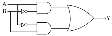
Q928 Jan 2025 · Shift 1MCQ
Which of the following circuits has the same output as that of the given circuit?
Figure for the question
  1. A
    Figure for the question
  2. B
    Figure for the question
  3. C
    Figure for the question
  4. D
    Figure for the question
Q1029 Jan 2025 · Shift 2MCQ
The difference of temperature in a material can convert heat energy into electrical energy. To harvest the heat energy, the material should have
  1. A
    low thermal conductivity and high electrical conductivity
  2. B
    high thermal conductivity and high electrical conductivity
  3. C
    high thermal conductivity and low electrical conductivity
  4. D
    low thermal conductivity and low electrical conductivity